My DIY HF SSB transceiver project began in 1988 with the first one, and with repeated improvements I have now completed my sixth one.
Whenever I make something, I always think that it is the best possible result, but when I finish it, I find that there is a part that bothers me. I should have stopped at that point, but I am a perfectionist by nature, and before I know it, I end up making an improved version.
Looking back now, I am astonished at myself for continuing to make 21MHz transceivers without any remorse.
QRP operations also include 50 MHz and 28 MHz, but it is unlikely that you will be able to find contacts on either of these frequencies outside of the summer E-sports season.
Furthermore, 50 MHz is a weak signal area in our area due to the presence of TV channel 2 broadcast waves. Because of this, TV interference occurs even if the radio clears the 60 dB spurious noise limit set by the Radio Law. For this reason, I'm interested in 50 MHz, but I haven't built one myself.
I've gone off on a tangent, but now I'll get to the main topic and explain the outline of Unit 6. Unit 6 has the following general improvements over its predecessor, Unit 5:
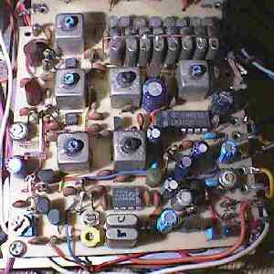
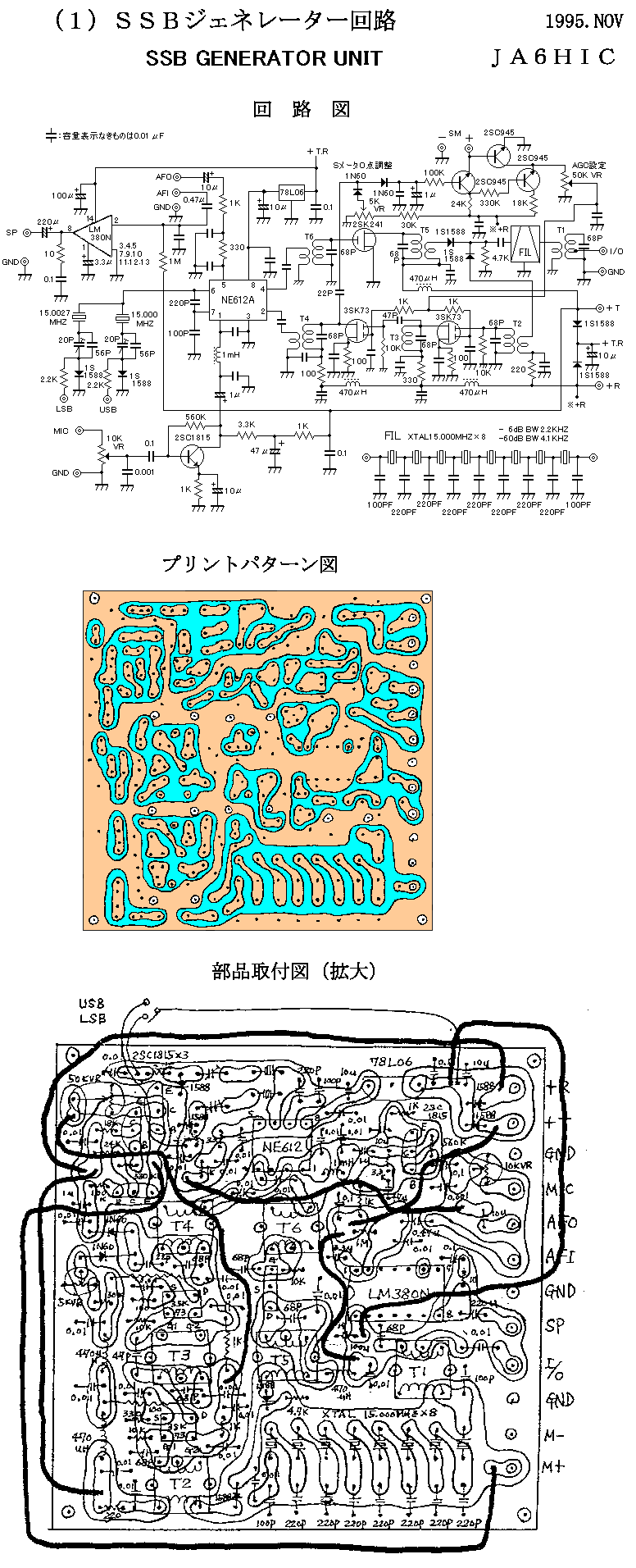
The NE612A was used for modulation and demodulation of the SSB generator.
The current consumption of the NE612A is only 2.5mA at a power supply voltage of 6V. Compared to the approximately 20mA consumed by the SN76514 used in Unit No. 5, this is a surprisingly low current consumption.
The maximum input frequency is 500MHz, which is an outstanding feat. Incidentally, the maximum input frequency on the local oscillator side is also 200MHz.
There is no way to not use such an excellent IC. Perhaps because I used it at only about 15MHz, even though it can be used up to 500MHz, it seems to be able to obtain sufficient carrier suppression without adding a carrier balance adjustment circuit.
It is now possible to output both USB and LSB.
When using a transverter to operate on other bands, the LSB may be required due to heterodyne.
This No.6 unit has two crystals for carrier oscillation, and can output either USB or LSB by switching with a switch. The carrier point frequency is set to 15.000 MHz for USB and 15.0027 MHz for LSB.
![]()
NE612A was used for the mixer of transverter
The transceiver( From NO1 to NO5 ) that I made in the past was using all the diode mixer for the mixer circuit.
A diode mixer has a very more excellent characteristic in respect of linearity and noise, in comparison with the active type mixer that used the transistor and FET.
As for the bad point of the diode mixer that the local oscillator (L0) the input is necessary as 10mW and the conversion gain be minus.
I used NE612A for the mixer of transverter in this NO6 machine aiming at the gain improvement of the reception system.
It is conceivable that the gain up that by means use NE612A becomes the gain up of about 20dB in comparison with the diode type mixer. As for this the mixing gain of NE612A the mixing gain of plus 14dB and, diode mixer are minus 6dB. When I think these comprehensively it becomes the gain up of plus 20dB.
When I try to receive it actually with this NO6 transceiver a clear gain up felt it from the movement of the S meter. Thus whether there was a change in the transformation characteristic of this machine is indefinite, the deterioration regarding SN did not feel.
AGC was operated even to high frequency amplifier stage.
The problem happened to the action in AGC to only IF stage along with the gain up of the reception system. So that AGC is left the action to high frequency stage as this measure the circuit was changed.
Lost the straight amplifier of the local oscillator inside transverter.
As for the input of the local oscillator of NE612A the power is not more necessary in comparison with the diode mixer. The straight amplifier of the local oscillator that I was inserting in a circuit from such a reason, became unnecessary. The parts decrease only the minute of a straight amplifier and the circuit became simple the result as.
A consumption current became without a balance change, because the consumption current of NE612 was added, although the consumption current of a straight amplifier became a zero.
![]()
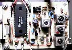
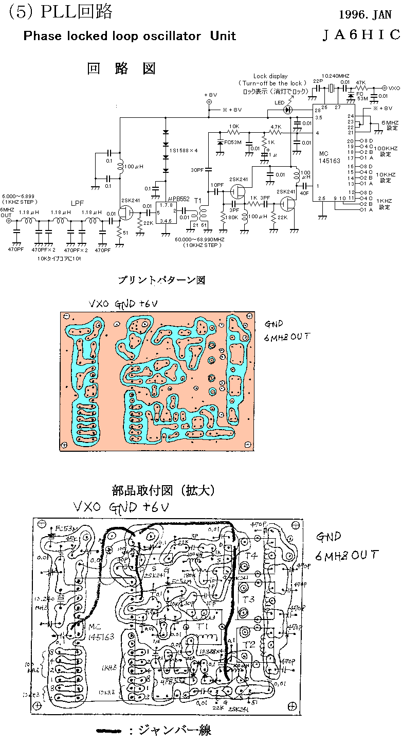
1/10 division IC of the PLL circuit were changed to uPB552.
The current flows, to HD10551 that was used conventionally in the PLL circuit of about about 60mA.
Because the decrease of the consumption current of integration is aimed at this time, it does the same action as HD10551 of division IC and there are greatly few consumption currents and be adopting uPB552.
The consumption current of uPB552 is only 6mA at the time of power supply voltage 6V! It is 1/10 low consumption currents compared with HD10551.
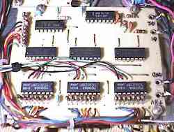
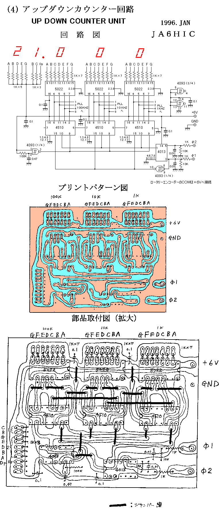
It makes the dial circuit and up down counter circuit one board
The NO5 transceiver was making dial encoder circuit and up down counter circuit each separately. This NO6 transceiver merged these two circuits to one board.
At first, I tried to create a flip-flop circuit using NAND, aiming to reduce the number of ICs by two overall, but counting errors occurred occasionally, so I changed to the current circuit.
In the current circuit, two NANDs and one and a half flip-flops are unused, which is a shame, but I have accepted that it is unavoidable for stable operation. In the end, by merging the two boards, the total number of ICs reduced by only one.
Here again, my obsessive nature got in the way (?), and I ended up getting completely bogged down in computer-related issues as I had to set up my computer environment and prepare to connect to the Internet.
Although Unit 6 is not yet complete, all that remains is to put it in its case. The main goal of this improvement was to reduce current consumption, and the results have been roughly as expected. Regarding this, I plan to create a comparison table with Unit 5, including current consumption, carrier suppression, and spurious generation values.
I am also considering changing the local oscillator to a DDS, and have already purchased a DDS kit from Akizuki Electronics. However, even if I assemble the kit as is, it will likely be difficult to use as a radio, so I plan to make a separate control circuit.
For this reason, we do not know what form No. 6 will take in its final completion, but for the time being it functions properly as a radio, so we have introduced it as a work in progress.
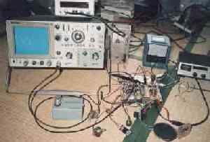
Observing two-tone waveform
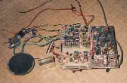
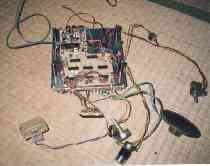
Top board layout status Bottom board layout status
 Return to the homepage